HX2272 Remote decoder circuit: Difference between revisions
| Line 12: | Line 12: | ||
==2. Features== | ==2. Features== | ||
*Low-power CMOS technology | *Low-power CMOS technology | ||
*SNR | * Low SNR | ||
* 6 Data | * Up to 12 Tri-State code addresses pins | ||
* Up to 6 Data pins | |||
*Operating voltage range: 3 to 18V | *Operating voltage range: 3 to 18V | ||
*Instantaneous output latch | *Instantaneous output latch | ||
*DIP package | *DIP package | ||
*RC oscillator | *RC oscillator | ||
==3 Applications== | ==3 Applications== | ||
Revision as of 01:40, 28 December 2007
<google>ENGELSK</google>
1. Description
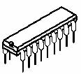
HX2272 is a remote control decoder for decoding signals encoded by the HX2262 Remote encoder circuit. The chipset is using CMOS technology. It has 12 bits of tri-state address pins providing a maximum of 531,441 (or 312) address codes; thereby, drastically reducing any code collision and unauthorized code scanning possibilities. HX2272 is available in several options to suit every application need : variable number of data output pins, latch or momentary output type.
2. Features
- Low-power CMOS technology
- Low SNR
- Up to 12 Tri-State code addresses pins
- Up to 6 Data pins
- Operating voltage range: 3 to 18V
- Instantaneous output latch
- DIP package
- RC oscillator
3 Applications
- Car security system home security / automation system
- Garage door controller
- Fans remote home security / automation systems
- Industrial remote control
- Toys with remote control
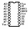
4. Pinout
| Pinout 18-lead package |
Pin name | Input/Output | Note | |
|---|---|---|---|---|
| 1 ~ 6 | A0 ~ A5 | I |
Code Address Pin Nos. 0 ~ 5. These six tri-state pins are detected by HX2272 to determine the encoded waveform bit 0 ~ bit 5. Each pin can be set to “0”, “1”, or “f” (floating). | |
| 7 ~ 8 10 ~ 13 |
A6/D5 ~ A11/D0 | I/O |
Code Address Pin Nos. 6 ~ 11/Data Pin Nos. 5 ~ 0. These six pins are used as higher address input bits or data output pins depending on the version (type) of HX2272 used. When used as address inputs, these pins are tri-state input pins and each pin can be set to “0”, “1”, or “f” (floating). When used as output pins, these pins are driven to VCC if (1) the address decoded from the waveform that was received matches the address setting at the address input pins, and (2) the corresponding data bits received is a “1” bit. Otherwise, they are driven to VSS. | |
| 14 | DIN | I |
Data Input Pin. The encoded waveform received is serially fed to HX2272 at this pin. | |
| 15 | OSC1 | I |
Oscillator Pin No.1 |
A resistor connected between these two pins determine the determine the basic HX2272 oscillation frequency. |
| 16 | OSC2 | O |
Oscillator Pin No.2 | |
| 17 | VT | O |
Valid Transmission. Active High Signal. VT in high state signifies that HX2272 receives valid transmission waveform. | |
| 18 | Vcc | -- | Power positive | |
| 9 | Vss | -- | Power negative | |
<google>ENGELSK</google>


